 |

 | Surface Quality Control for Maximizing LIDT in High-PowerLaserOptics 06 Oct Optoman in collaboration with Dioptic In high-power laser systems, the optical components' resilience to laser-induced damage directly determines performance, reliability, and service life. Even minor surface or subsurface imperfections can severely compromise the laser-induced damage threshold (LIDT), introducing failure points that limit system capability. |
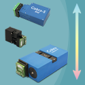 | Choosing the best spectrometer for NIR OCT 02 Apr Wasatch Photonics Near infrared optical coherence tomography has traditionally been limited to imaging depths of just a few millimeters, but with our expanded line of OCT spectrometers, up to 12 mm is possible. In this tech note, we explore and compare three different drop-in spectrometer models designed to serve a wide range of resolution, depth, and size requirements in NIR OCT imaging. |
 | Harnessing Einstein’s Photoelectric Effect: Advancements in LiDAR Technology and Its Impact on Modern Sensors 26 Aug Hamamatsu Photonics Europe Hamamatsu Photonics is leading the evolution of LiDAR with advanced sensor technologies that enhance precision and reliability. Their Time-of-Flight systems, based on Einstein’s photoelectric effect, use rapid laser pulses and sophisticated detectors - Avalanche Photodiodes (APDs) and Silicon Photomultipliers (SiPMs) - to capture real-time distance data with exceptional accuracy. Optimized for thermal stability and energy efficiency, these sensors are ideal for autonomous vehicles, robotics, and smart devices. Hamamatsu’s continued innovation in APD and SiPM technologies is accelerating the integration of intelligent systems into everyday life. |
 | Identifying Optical Materials with Precision Accuracy 04 Mar Knight Optical Precision accuracy is a critical necessity with any optical component. Rigorous testing to ensure strict compliance with given requirements will always be essential; it is a vitally important demand within any industry sector. Dimensional, surface profiling and optical performance testing are significant aspects of this process, but an additional layer of assurance and quality can be achieved with the use of material verification, employing methods such as refractive index, density testing and transmission measurement. This White Paper explores advanced techniques for precise optical material verification, overcoming the limitations of traditional testing methods. |
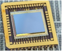 | NRC’s Photodetector Activities in the Short-Wavelength Infrared 14 Aug National Research Council Canada III-V compound semiconductors are the most efficient solid state light emitters and photodetectors. They are the backbone of the laser and detector technologies underpinning optical fibre telecommunications. In addition, for state-of-the-art imaging applications,). The National Research Council of Canada (NRC) has developed extensive capabilities in terms of design, epitaxy, fabrication, and testing of both laser and detector device structures, such as large area focal plane photodetector arrays (FPAs) in the short-wavelength infrared (SWIR: 1.0-1.7 µm range). |
 | Achieving Clean Pulses (Picosecond) and Stable CW with 1 µm DFB Seed Lasers 25 Jul QD Laser Fiber lasers and solid-state / fiber hybrid lasers using rare earth doped fiber or crystal are expected to be widely used in various industrial applications such as semiconductor inspection equipment, micromachining, LiDAR, etc., due to their compactness and robustness. QD Laser developed and produced 1 µm band wavelength semiconductor DFB (Distributed FeedBack) lasers, which can be used for seed light sources of these lasers, by utilizing crystal growth technology, grating formation technology, and semiconductor laser chip design technology. We will introduce the features of our DFB lasers. |
 | Overcoming Thermal and Optical Feedback Challenges with 1310 nm Quantum Dot Lasers 25 Jul QD Laser Semiconductor lasers in a wavelength range around 1310 nm are widely used as light sources for intra- and inter-data center optical communications. In recent years, it has also been introduced as a light source for silicon photonic circuits called silicon photonics. In addition, a new application of silicon photonics “LiDAR” is emerging to realize autonomous driving and advanced robotics. The requirements for semiconductor lasers for these applications are high reliability in high temperature environments and high tolerance against external optical feedback. We are developing and manufacturing quantum dot lasers that can meet these demands. |
 | Advancing Biomedical Applications with Miniaturized, Energy-Efficient Lasers (532/561/594 nm) 25 Jul QD Laser QD Laser developed and produced patented 532, 561 and 594 nm compact visible lasers in which a semiconductor DFB laser and nonlinear crystal are integrated in a small flat package. Since the linewidth of DFB laser is several MHz due to high selectivity of gratings for lasing wavelength, the visible light converted by nonlinear crystal is also single frequency with narrow linewidth. In addition, the optical power stability is high because high stability of optical power generated by DFB laser is directly transferred to the visible light. This enables improvement of detection accuracy and resolution of an object. |
 | Greener Industry with Advanced Gas Detection 01 Jul Hamamatsu Photonics Europe Hamamatsu Photonics is advancing industrial sustainability with cutting-edge infrared solutions tailored for real-time emissions monitoring. Supporting critical applications such as continuous emissions monitoring systems and leak detection and repair programs, Hamamatsu’s photonics technology enables industries to meet strict environmental regulations while improving detection accuracy, operational efficiency, and responsiveness in emission control. |
 | Transforming Free-Space Data Transmission in Rotary Joints 29 May Hamamatsu Photonics Europe Hamamatsu Photonics explores how the latest optical transceiver facilitates free-space data transmission in rotary joints, eliminating the vulnerabilities of optical fibers. This innovation offers advantages such as bidirectional communication, high-speed data transfer, and robust performance in challenging environments. Key applications include rotating cameras, medical devices, and automotive systems, positioning the transceiver as a vital asset for advanced industrial applications. Read the full article now! |
 | Distribution of light means the distribution of information: the use of piezo technology for optical fiber switches 29 May piezosystem jena GmbH Discover the future of optical signal processing: piezoelectric fiber optic switches enable ultra-fast, precise and energy-efficient switching of light signals, for example for bundling process currents. Ideal for quality assurance, measurement technology and laser technology - with minimal signal loss and maximum reliability. Benefit from a compact design, long service life and the latest innovations for demanding applications in research and industry. |
 | Laser Sintering Technology: The Future of Printed Electronics 02 May Hamamatsu Photonics Europe Laser sintering is a relatively new technology that uses lasers as efficient thermal energy sources for sintering metal particle-based inks. Discover how Hamamatsu Photonics has been assisting the printed electronics industry through extensive testing, with the support of partners, to find the optimal sintering conditions for different ink and substrate combinations. |
 | CMOS and its application in spectroscopy 19 Mar Hamamatsu Photonics Europe Explore the technology behind CMOS sensors and their increasing popularity in spectroscopy techniques. Thanks to their energy efficiency and easy integration, Hamamatsu Photonics’ CMOS image sensors are adapted to meet the evolving applications of water analysis, food inspection, and industrial position detection. Learn more about how Hamamatsu’s CMOS technology is aiding industrial, analytical, and spectroscopy markets |
 | Photodiodes Exposed: Unlocking the characteristics of these crucial sensors 21 Feb Hamamatsu Europe Photodiodes. Uncover why their characteristics, such as high sensitivity and low dark current, make them a crucial type of sensor in applications such as medical and scientific measurements, analytical, fire safety, optical communications, photovoltaics, and automation. |
| © 2025 SPIE Europe |
|


