

Article summary
AI generated
Low-noise amplifiers (LNAs) are essential for enhancing signal quality in wireless sensor networks, where performance metrics like gain, noise figure, and power consumption must be optimized under manufacturing variations. This study successfully integrates Latin Hypercube Sampling with the Non-Dominated Sorting Genetic Algorithm III to achieve significant improvements in a 45 nm CMOS LNA, resulting in a 49.2% reduction in noise figure, a 27.3% increase in voltage gain, and a 35.2% decrease in power dissipation, while ensuring robustness against process-induced variations.
Abstract
Low-noise amplifiers (LNAs) are critical components of wireless sensor network (WSN) receivers, where high gain, low noise, low power consumption, and robust operation under process variations are essential. This study presents a variation-aware multi-objective optimization framework for a 45 nm CMOS LNA by integrating Latin Hypercube Sampling (LHS) with the Non-Dominated Sorting Genetic Algorithm III (NSGA-III). Process-induced variations in threshold voltage, channel length, oxide thickness, electron mobility, and gate capacitance are modeled using statistically representative LHS samples and incorporated directly into the optimization process. Four key RF performance metrics—noise figure (NF), voltage gain, power dissipation (PD), and third-order input intercept point (IIP3)—are optimized simultaneously. The optimized design achieves an NF of 1.32 dB, gain of 15.40 dB, PD of 0.59 mW, and IIP3 of 3.8 dBm, demonstrating substantial improvements over the baseline design. Additional RF validation through S-parameter, stability, noise figure, and two-tone intermodulation analyses confirms the practical effectiveness of the optimized LNA. The results show that the proposed LHS–NSGA-III framework can generate robust Pareto-optimal solutions under manufacturing uncertainties, providing an effective methodology for designing energy-efficient and reliable RF front-end circuits for emerging WSN and IoT applications.
1 Introduction
The rapid expansion of wireless sensor networks (WSNs) has revolutionized the landscape of low-power and distributed sensing applications, ranging from environmental monitoring and industrial automation to healthcare and smart cities [1, 2]. Central to the performance of these networks is the efficiency and sensitivity of their front-end radio frequency (RF) components, especially the low noise amplifier (LNA), which serves as the first active stage in the receiver chain [3, 4]. LNAs are responsible for amplifying weak incoming signals while introducing minimal additional noise, thereby directly influencing the signal-to-noise ratio (SNR) and, consequently, the overall communication reliability of WSN nodes [5].
As CMOS technology continues to scale into nanometer dimensions, particularly below 65 nm, several benefits such as increased integration density, reduced area, and lower power supply requirements have emerged [5, 6]. However, this miniaturization is accompanied by significant challenges, especially for analog and RF circuits [5]. Key among these are process-induced variations in parameters like threshold voltage \({(V}_{th})\), channel length (L), oxide thickness \({(T}_{ox})\), and mobility \({(M}_{n})\), which introduce uncertainty in circuit behavior and degrade yield and robustness [7, 8]. In sub-100 nm nodes, these variations can result in substantial shifts in gain, noise figure, power consumption, and linearity of LNAs, complicating the design optimization process [9].
Traditional analog design methods often rely on iterative simulations and designer intuition to meet multiple conflicting objectives [10]. However, these approaches fall short in high-dimensional, nonlinear, and variation-prone design spaces [11]. To address these limitations, metaheuristic optimization techniques such as genetic algorithms (GA), particle swarm optimization (PSO), and differential evolution (DE) have been employed in recent years [12, 13]. While effective in exploring large solution spaces, many of these techniques either lack the ability to handle multiple objectives simultaneously or suffer from issues related to diversity loss and convergence stagnation, particularly when faced with stringent analog design constraints [14, 15].
The non-dominated sorting genetic algorithm III (NSGA-III), a recent advancement in the family of evolutionary algorithms, offers a promising solution for handling many-objective optimization problems [16]. Its ability to maintain a well-distributed Pareto front using predefined reference points makes it highly suitable for analog circuit optimization, where trade-offs between multiple performance metrics such as noise figure (NF), gain \({(A}_{v})\), power dissipation (PD), and third-order intercept point \({(IIP}_{3})\), must be carefully balanced [17]. Despite its strengths, a critical gap in literature remains in incorporating statistical process variations into NSGA-III-based design flows for LNAs.
To ensure statistical robustness under manufacturing uncertainties, the LHS has been adopted as a highly efficient and stratified method for generating representative samples of process parameters [18]. Unlike traditional Monte Carlo methods, LHS ensures uniform coverage of the parameter space with fewer simulations, making it ideal for high-cost analog circuit evaluations [19].
This paper presents a robust multi-objective optimization framework for the design of a 45 nm CMOS low-noise amplifier (LNA) intended for wireless sensor network (WSN) applications. The proposed approach integrates Latin Hypercube Sampling (LHS) with NSGA-III to simultaneously account for manufacturing variability and optimize circuit performance. Key process parameters, including threshold voltage, channel length, oxide thickness, mobility, and gate capacitance, are incorporated into the design framework, while four critical RF performance metrics—noise figure (NF), voltage gain, power dissipation (PD), and third-order input intercept point (IIP3)—are optimized concurrently. Through comprehensive statistical validation, benchmarking, and sensitivity analysis, the proposed methodology demonstrates its ability to generate robust Pareto-optimal solutions under realistic process uncertainties. By jointly addressing reliability and performance trade-offs, this work provides a practical design framework for energy-efficient and resilient RF front-ends in emerging WSN and Internet of Things (IoT) applications. The remainder of the paper is organized as follows. Section 2 reviews the relevant literature and identifies the research gap. Section 3 describes the LNA circuit design and modeling methodology. Section 4 presents the process variation modeling approach using LHS. Section 5 details the NSGA-III-based multi-objective optimization framework. Section 6 discusses the results and validation, and Sect. 7 concludes the paper with recommendations for future research.
2 Literature review
2.1 CMOS LNA topologies for WSN
The LNAs form the cornerstone of RF front-ends in WSNs, where energy efficiency, sensitivity, and compactness are critical [20]. Among various topologies, the common-source inductive degeneration LNA remains the most widely adopted configuration due to its superior input matching and low noise performance [21]. This topology enables a trade-off between gain and noise figure (NF), while ensuring adequate linearity and power efficiency [22, 23]. For WSN applications, the challenge lies in optimizing these trade-offs under constrained power budgets, typically below 1 mW [24]. While cascode LNAs offer higher gain and isolation, they often suffer from increased power consumption and reduced linearity in scaled CMOS technologies [25]. Thus, most recent studies have focused on simplified yet robust topologies suitable for integration with digital baseband processing in modern system-on-chip designs [26,27,28].
2.2 Challenges of process variability in sub-100 nm CMOS
As CMOS technology scales into deep submicron regions (< 100 nm), process-induced variations such as fluctuations in threshold voltage \(({V}_{th})\), channel length (L), oxide thickness \(({T}_{ox})\), and carrier mobility \(({M}_{n})\), have become major sources of performance uncertainty in analog circuits [29, 30]. These statistical variations, resulting from lithographic limitations and material inconsistencies, significantly degrade yield and reliability, especially for sensitive analog blocks like LNAs [31, 32]. In particular, variability in \({V}_{th}\) impacts the transconductance (\({g}_{m}\)), which in turn affects gain and NF [33]. Similarly, variations in \({T}_{ox}\) influence gate capacitance and biasing points, making the design highly sensitive to manufacturing corners [34,35,36]. While digital designers have adopted design-for-yield (DfY) strategies, such systematic approaches are less prevalent in analog design, largely due to the complexity of modeling nonlinear behaviors under stochastic perturbations [37,38,39,40].
2.3 Overview of analog optimization techniques
To address the complex trade-offs involved in LNA design, several metaheuristic optimization algorithms have been adopted over the past decade [41, 42]. The genetic algorithms (GA), particle swarm optimization (PSO), simulated annealing (SA), and differential evolution (DE) have been particularly popular due to their global search capability and ease of implementation [43, 44]. These methods have been used to optimize parameters like gain, NF, and power consumption. However, many of these approaches fall short in simultaneously addressing all performance objectives and often neglect the influence of process variations [45, 46]. Table 1 summarizes key contributions in this domain. For example, Kouhalvandi [47] used PSO on a 90 nm node but did not consider variability, while a previous study [26] employed NSGA-II but suffered from diversity loss. Most methods either optimize only one or two objectives or lack statistical robustness, limiting their applicability to modern sub-100 nm design contexts [26, 38, 39, 48].
2.4 Role of sampling methods in statistical modeling
Given the inherent process variability, statistical modeling has become an essential aspect of modern analog design flows [35]. The LHS has emerged as a powerful technique for generating representative samples across multidimensional distributions with fewer simulations compared to traditional Monte Carlo methods [18]. LHS ensures stratified and uniform sampling, enabling efficient exploration of the design space under uncertainty [28, 40]. Despite its advantages, LHS has rarely been integrated with multi-objective optimization workflows in analog RF circuits [27]. Most prior works rely on fixed process corners or simplistic Gaussian perturbations without comprehensive statistical treatment, resulting in non-robust designs vulnerable to yield loss [34, 36].
2.5 NSGA-III in multi-objective RF circuit design
NSGA-III, the third generation of non-dominated sorting genetic algorithms, represents a major advancement in solving multi-objective problems with more than three conflicting goals [37,38,39]. It introduces a reference-point-based selection strategy that ensures a diverse and well-distributed Pareto front [54]. In RF circuit design, where trade-offs among gain, NF, PD, and IIP3 are highly nonlinear and interdependent, NSGA-III provides a structured approach to identify optimal compromises. Although Lberni et al. [29] applied NSGA-III for LNA design at 7 nm, their study did not incorporate process variation modeling. The true potential of NSGA-III remains underutilized in the analog domain, particularly when combined with LHS-based uncertainty modeling to ensure robust performance [37, 48].
Table 1 highlights major studies in LNA optimization over the past decade, mapping the CMOS node, optimization approach, targeted objectives, and associated limitations. It is evident that while earlier works like those of Kouhalvandi [47] and Ghanevati [55] focused on PSO and GA respectively, their scope was narrow—addressing either gain or NF with no consideration of process variability. More recent efforts, such as Roobert and Rani [14] and Kumar and Deolia [52], employed advanced algorithms like NSGA-II and NSGA-III but were limited in terms of constraint handling or robustness evaluation. Notably, none of the reviewed studies integrate both variation-aware sampling (e.g., LHS) and multi-objective optimization in a unified workflow [34, 40, 53]. This underscores the novelty and need for the proposed LHS-NSGA-III framework, which addresses all four primary metrics (NF, Gain, Power, IIP3) while ensuring statistical design robustness.
3 Research gap and novel contribution
Despite significant advances in the application of metaheuristic algorithms for analog circuit design, several important challenges remain unresolved. Most existing studies optimize only a limited set of RF performance metrics and rarely consider noise figure (NF), voltage gain, power dissipation (PD), and third-order input intercept point (IIP3) simultaneously within a unified framework [34, 35]. Furthermore, process-induced variations inherent in deep-submicron CMOS technologies are often neglected during optimization, resulting in designs that perform well under nominal conditions but exhibit reduced reliability under manufacturing uncertainties. Although algorithms such as NSGA-II and NSGA-III have demonstrated strong capabilities in multi-objective optimization, their integration with statistically representative sampling techniques for variation-aware design remains limited [36, 40]. In addition, many reported optimization studies focus primarily on performance enhancement without systematically evaluating robustness and sensitivity to process fluctuations [56, 57]. To address these gaps, the present study develops a variation-aware optimization framework that integrates Latin Hypercube Sampling (LHS) with NSGA-III for CMOS LNA design in 45 nm technology. The proposed methodology simultaneously optimizes NF, gain, PD, and IIP3 while incorporating process-induced variability directly within the optimization loop. Furthermore, extensive statistical validation using 1000 LHS-based Monte Carlo samples and sensitivity analysis of key process parameters are performed to evaluate design robustness under realistic manufacturing conditions. By combining statistical variation modeling with many-objective optimization, this work provides a practical framework for the design of high-performance, energy-efficient, and robust RF front-end circuits for emerging wireless sensor network (WSN) and Internet of Things (IoT) applications.
4 LNA circuit design and modeling
4.1 Selection of LNA topology
The design of a LNA for WSNs necessitates a topology that offers an optimal balance between gain, noise figure, linearity, and power consumption. Among various configurations, the common-source inductive degeneration topology is widely regarded as the most effective solution in sub-100 nm CMOS processes. This topology not only facilitates real input impedance matching through a source inductor (\({L}_{s}\)), but also significantly enhances the noise performance by suppressing the input-referred thermal noise. Additionally, it enables ease of integration and minimal complexity, which are essential for compact, low-power applications like WSNs.
Figure 1 schematic of the common-source inductive degeneration LNA used in this study. The design employs cascaded NMOS transistors (Q2 and Q3) with source degeneration (LS) for improved matching and linearity. Input matching is achieved via L1 and R2, while Q2 functions as an active load with output resonance formed by LG and CL. Biasing is provided through Vg1, Vg2, RB, and bypass capacitor CEX. This topology is optimized for low-power, high-gain WSN applications under process variations.

Schematic of Common-Source Inductive Degeneration LNA
4.2 Technology and design parameters
The simulation and optimization are performed using a 45 nm CMOS technology node, chosen for its balance between process maturity and feature scaling. Table 2 summarizes the key physical and electrical parameters used in the simulation environment. A supply voltage (VDD) of 1.0 V is adopted to meet low-power constraints. The minimum channel length (\({L}_{min}\)) of 45 nm ensures high-frequency operation, while the oxide thickness (\({T}_{ox}\)) of 1.2 nm influences the gate capacitance and threshold behavior. Electron mobility (\({M}_{n}\)), set to 250 cm2/V·s, governs the transconductance, while the nominal threshold voltage (\({V}_{th}\)) of 0.28 V defines the biasing conditions.
An initial channel width (\({W}_{init}\)) of 300 nm is chosen for pre-optimization simulation. The gate oxide capacitance per unit area (\({C}_{ox}\)), approximately 7.2 × 10⁻3 F/m2, impacts high-frequency response and input impedance. The thermal voltage (\({V}_{T}\)) is taken as 26 mV at room temperature (300 K). These parameters form the foundation for both schematic-level simulation and variation-aware modeling.
4.3 Performance metrics and expressions
In CMOS LNA design, particularly for WSNs in nanometer technologies, the following four performance metrics are critically evaluated and jointly optimized:
a) Voltage Gain (\({A}_{v}\)): The small-signal voltage gain for a common-source LNA with source degeneration is given by:
where, \({g}_{m}\) is the transconductance of the MOS transistor (≈ \(\frac{2{I}_{D}}{{V}_{ov}}\)), \({R}_{L}\) is the effective load resistance (typically includes output inductor \({L}_{Load}\)), and \({R}_{S}\) represents the source degeneration resistance or impedance from inductor \({L}_{S}\). Maximizing \({A}_{v}\) is critical to enhancing the amplifier’s signal gain while maintaining linear operation. A well-optimized voltage gain improves the receiver's sensitivity, reduces the noise contribution from subsequent stages, and enables efficient signal processing with minimal distortion.
b) Noise Figure (NF): The noise figure (NF) quantifies the degradation of the signal-to-noise ratio (SNR) introduced by the amplifier. It is a critical metric in determining the sensitivity of RF front-end circuits. For a MOSFET-based LNA employing source degeneration, the noise figure is expressed as:
where, γ is the excess noise coefficient (≈ 2/3 for long-channel devices), and \({g}_{m}\), \({R}_{S}\) as defined above. Minimizing NF is essential for achieving high-quality signal reception, particularly in environments characterized by low signal strength or high levels of ambient noise. A lower NF leads to enhanced receiver sensitivity and improved overall system performance in WSNs and other low-power RF applications.c) Power Dissipation (\(PD\)): Power dissipation is a critical consideration in the design of LNAs for portable and battery-powered applications, such as WSNs and IoT devices. The total power consumed by the LNA is given by:
where, \({V}_{DD}\) is the supply voltage, and \({I}_{D}\) is the drain bias current. Minimizing \({P}_{D}\) is essential to extend battery life, reduce thermal stress, and enable long-term operation in energy-constrained environments. An energy-efficient LNA design ensures sustainable performance without compromising gain or signal fidelity.
d) Third-Order Input Intercept Point (3): The IIP3 is a key metric that quantifies the linearity of an RF amplifier. It represents the hypothetical input power level at which the power of third-order intermodulation distortion (IMD3) products equals the power of the fundamental signal components. Mathematically, IIP3 is inversely proportional to the third-order nonlinearity coefficient:
where: \({a}_{3}\) is the third-order nonlinearity coefficient in the Taylor series expansion of the amplifier’s input–output behavior. In practical RF design, IIP3 is typically obtained through two-tone large-signal simulations, where the nonlinear behavior of the amplifier under closely spaced frequency tones is observed. Maximizing IIP3 is critical for minimizing signal distortion and intermodulation, especially in environments with high levels of adjacent-channel interference. A high IIP3 ensures that the LNA maintains signal fidelity even when exposed to strong interfering signals, making it highly suitable for dense wireless systems and multi-channel receivers.
Figure 2 small-signal equivalent model of the common-source inductive degeneration LNA. The input signal \({V}_{in}\) is applied through the gate inductor \({L}_{g}\), and the gate-source capacitance \({C}_{gs}\) forms part of the resonant input network. Source degeneration is implemented via \({L}_{s}\), improving input matching and linearity. The transistor is modeled by the controlled current source \({g}_{m}\).\({V}_{gs}\), and the output is tuned using the drain inductor \({L}_{d}\). This model is used for analyzing gain, noise, and impedance behavior in the LNA.
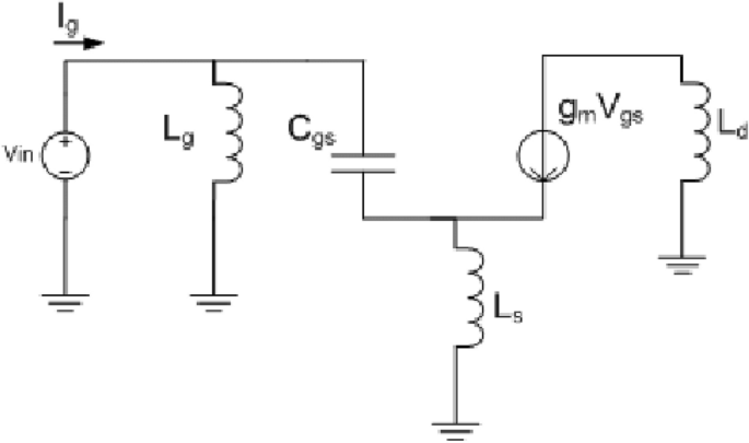
Small-Signal Equivalent Model of the LNA
5 Parametric variation modeling using LHS
5.1 Motivation for LHS
Process-induced variability in deep submicron CMOS technologies significantly impacts the performance and reliability of analog circuits. In RF front-ends such as LNAs, variations in threshold voltage (\({V}_{th}\)), channel length (L), oxide thickness (\({T}_{ox}\)), and other key parameters can result in substantial deviations in gain, noise figure, and linearity. To model these effects efficiently and accurately, the LHS is employed in this study. LHS ensures uniform and stratified sampling across the distribution range of each input variable, outperforming conventional random sampling by providing better statistical coverage with fewer required samples [58]. This leads to more accurate and robust performance evaluation under manufacturing uncertainties.
5.2 Parameter selection and statistical distributions
The process parameters considered for variation modeling include threshold voltage (\({V}_{th}\)), channel length (\(L\)), oxide thickness (\({T}_{ox}\)), electron mobility (\({\mu}_{n}\)), and gate oxide capacitance per unit area (\({C}_{ox}\)). These parameters were selected because of their significant influence on transconductance (\({g}_{m}\)), input matching, noise performance, linearity, and high-frequency behavior of the low-noise amplifier (LNA). Variations in these parameters can substantially affect circuit performance and yield in deep-submicron CMOS technologies. Table 3 summarizes the nominal values, standard deviations, variation ranges, statistical distributions, and their corresponding impacts on LNA performance.
The selected statistical distributions are based on commonly reported process variability characteristics in deep-submicron CMOS technologies. Threshold voltage (\({V}_{th}\)), oxide thickness (\({T}_{ox}\)), electron mobility (\({\mu}_{n}\)), and gate capacitance (\({C}_{ox}\)) were modeled using Gaussian distributions because these parameters are influenced by multiple independent fabrication mechanisms, resulting in approximately normal statistical behavior. In contrast, channel length (\(L\)) was represented using a bounded uniform distribution to capture lithographic and etching uncertainties within specified fabrication tolerances [56]. The present study primarily considers global process variations, which affect all devices similarly and represent a dominant source of manufacturing uncertainty during early-stage design optimization. However, local mismatch effects, such as random dopant fluctuations and device-to-device variations, were not explicitly modeled. Similarly, statistical correlations among process parameters were not incorporated due to the absence of foundry-specific covariance data for the selected 45 nm technology node. Consequently, the adopted framework captures the dominant effects of global manufacturing variability while maintaining computational efficiency for large-scale statistical optimization. The resulting variation-aware model provides a realistic and statistically representative basis for evaluating the robustness of the optimized LNA under manufacturing uncertainties [57].
5.3 LHS algorithm and sampling strategy
The LHS is adopted to efficiently model process variations across multiple design parameters by ensuring uniform and stratified sampling of each variable's distribution [59]. To determine the appropriate number of samples, the standard heuristic is applied:
where N is the number of LHS samples and kk is the number of statistically varied parameters. In this study, with k = 6, a minimum of 60 samples is required. To enhance robustness and support accurate Monte Carlo analysis, 1000 LHS samples are used, providing comprehensive coverage of the variation space and ensuring reliable performance evaluation of the LNA under process-induced fluctuations.
Figures. 3 and 4 provide a visual comparison of the sampling quality achieved using LHS versus traditional random sampling for the key process parameters—threshold voltage (\({V}_{th}\)) and channel length (L). Figure 3 illustrates the two-dimensional projection of the LHS-generated sample space, clearly demonstrating a well-distributed, stratified pattern that uniformly spans the entire range of both \({V}_{th}\) and L. This ensures that all regions of the variation space are adequately represented, including the edges and corners that are typically under-sampled in random methods. In contrast, Fig. 4 highlights the superiority of LHS over conventional random sampling by juxtaposing their coverage patterns. The left subplot of Fig. 4 (LHS Sampling) shows a dense, grid-like distribution that maintains consistency across the range, while the right subplot (Random Sampling) reveals noticeable clustering in some regions and voids in others, particularly along the parameter boundaries. Such non-uniformity in random sampling can lead to biased performance estimation and incomplete exploration of corner cases during variability analysis. Therefore, LHS is preferred in this study as it enhances statistical reliability, improves Monte Carlo convergence, and ensures robust evaluation of the LNA under manufacturing-induced fluctuations.

2D Projection of LHS Sampling for Vth vs. L

Comparison of Coverage–LHS vs Random Sampling
6 Multi-objective optimization using NSGA-III
6.1 Problem formulation
6.1.1 Assumptions of the study
To maintain computational tractability and relevance to CMOS design rules, the following assumptions are made; (a) The LNA uses a common-source inductive degeneration topology; (b) Device models are extracted from PTM 45 nm predictive technology models; (c) Process parameter variations (e.g., \({V}_{th}\), \({T}_{ox}\), L) follow Gaussian or Uniform distributions based on foundry data; (d) All simulations are performed at room temperature (300 K); (e) Matching network parasitics are assumed negligible for initial optimization; layout parasitics are left for post-layout refinement; and (f) interconnect parasitics, package effects, substrate coupling, and post-layout extraction effects are not explicitly included in the optimization process. These assumptions enable efficient evaluation of design trade-offs and process-induced variability while maintaining a manageable computational burden. The potential influence of layout parasitics, package effects, and temperature variations on practical RF performance is discussed as a limitation of the present study and identified as an important direction for future work.
6.1.2 Design variables and bounds
The optimization of the CMOS LNA is performed by tuning six key design variables (see Table 4), each with defined physical and operational bounds based on the capabilities of the 45 nm CMOS technology. The transistor width (W) ranges from 100 to 500 nm and directly influences the transconductance (\({g}_{m}\)), which in turn affects gain, noise figure, and impedance matching. The channel length (L) is varied between 45 and 90 nm; increasing L can improve output impedance and gain-bandwidth product but may also impact power efficiency. The bias current (\({I}_{B}\)), ranging from 100 µA to 600 µA, determines the operating point of the LNA and influences power dissipation, linearity, and noise characteristics. Load inductance (\({L}_{load}\)) is varied from 0.5 nH to 2.5 nH and plays a crucial role in tuning the output resonance and enhancing voltage gain. The source degeneration inductance (\({L}_{s}\)) ranges from 0.1 nH to 1.0 nH, improving linearity and stability, though often at the cost of gain. Finally, the gate-to-source capacitance (\({C}_{gs}\)), varied between 20 and 100 fF, controls the input impedance and resonance behavior.
6.1.3 Objective functions
The LNA design problem is formulated as a multi-objective optimization task involving four conflicting performance metrics. The objectives include: (i) minimization of noise figure (NF) to ensure high sensitivity in low-signal environments, (ii) minimization of power dissipation \({(P}_{D}\)) to prolong battery life and thermal stability, (iii) maximization of voltage gain \({(A}_{v}\)) for improved signal amplification, and (iv) maximization of third-order input intercept point (IIP3) to enhance linearity and reduce distortion. The original optimization problem is expressed as:
Since NSGA-III inherently handles minimization problems, the maximization objectives are algebraically transformed by negating them, yielding:
This transformation enables the algorithm to identify Pareto-optimal trade-offs among these four key performance goals.
6.1.4 Constraints of the study
The optimization process is governed by two categories of constraints: design constraints, which ensure compliance with functional performance requirements, and process variation constraints, which account for manufacturing uncertainties in nanometer CMOS technology.
6.2 Design constraints
To meet the performance standards for WSN applications, the following specifications are enforced throughout the optimization process:
-
a)
Voltage Gain (\({A}_{v}\)) must be at least 14 dB to ensure adequate signal amplification.
-
b)
Noise Figure (NF) must not exceed 2.0 dB to maintain high receiver sensitivity in low-signal environments.
-
c)
Power Dissipation (PD) must be limited to 1.0 mW to support low-power and battery-operated nodes.
-
d)
Input Reflection Coefficient (\({S}_{11}\)) must remain below –10 dB, indicating acceptable impedance matching; although not directly optimized, this criterion is verified during post-optimization validation.
6.3 Process variation constraints
To ensure robustness against manufacturing-induced fluctuations, the design must remain resilient within ± 3σ statistical variations of key process parameters. These include; (a) Threshold voltage \({V}_{th}\); (b) Oxide thickness \({T}_{ox}\); and (c) Channel length L.
These variations are implicitly modeled through LHS, which enables stratified and statistically representative sampling of the multidimensional variation space. By incorporating these uncertainties into the optimization loop, the proposed methodology ensures that the resulting LNA configurations exhibit not only high performance under nominal conditions but also resilience and manufacturability across real-world process corners.
6.4 NSGA-III algorithm configuration
The NSGA-III algorithm is configured with parameters summarized in Table 5 to ensure effective exploration and convergence in the high-dimensional design space [60]. The algorithm starts with a population of 100 individuals and runs for 80 generations. Simulated Binary Crossover (SBX) with a probability of 0.9 and Polynomial Mutation with a probability of 0.1 are used to generate diverse offspring. Elitism is maintained through non-dominated sorting and reference point-based niching. A total of 92 structured reference points is uniformly distributed across the normalized objective space to guide elitist selection and preserve diversity.
Figure 5 illustrates the complete flowchart of the optimization framework adopted in this study, which combines LHS with NSGA-III for robust multi-objective design of the CMOS Low Noise Amplifier (LNA). The process begins with LHS-based initialization, where a parent population (\({P}_{o}\)) is generated along with H structured reference points (\({Z}_{s}\)) to ensure comprehensive coverage of parametric variations. Simulated Binary Crossover and Polynomial Mutation are then applied to produce an offspring population (\({O}_{o}\)), and a combined population (\({R}_{o}\) = \({P}_{o}\) ∪ \({O}_{o}\)) undergoes non-dominated sorting to extract the Pareto fronts (\({F}_{1}\), \({F}_{2}\), …, \({F}_{i}\)). If the size of the selected intermediate population (\({S}_{t}\)) does not meet the target (N), additional individuals are drawn from the last front (\({F}_{i}\)) based on proximity to structured reference points. Each objective function is normalized across the population using maximum and minimum values (\({Z}_{imax}\) and \({Z}_{imin}\)), and reference points are projected onto a normalized hyperplane to guide elitist selection. A niche count is calculated for each reference point, and K members are selected to ensure diversity in the next generation (\({P}_{t+!}\)). This cycle continues until a stopping criterion—typically a predefined number of generations—is reached. The result is a Pareto-optimal set of solutions that simultaneously minimize noise figure and power consumption while maximizing voltage gain and third-order linearity (IIP3), under statistically modeled process variation constraints. This algorithmic configuration ensures that the optimized designs are not only high-performing but also robust to sub-100 nm CMOS process uncertainties.

Flowchart of Optimization Using LHS + NSGA-III
6.5 Computational complexity analysis
The computational complexity of the proposed framework is primarily determined by the population size, number of generations, and objective-function evaluations [36]. With a population size of 100 and 80 generations, approximately 8000 candidate solutions are evaluated during optimization. The incorporation of 1000 LHS samples increases the computational burden associated with robustness assessment; however, it provides substantially better statistical coverage than conventional random Monte Carlo sampling for a comparable computational budget. Furthermore, the evaluation of candidate solutions is inherently parallelizable, making the framework suitable for implementation on modern multi-core and high-performance computing platforms. Such parallelization can significantly reduce optimization runtime while preserving solution quality and diversity.
7 Results and discussion
7.1 Performance before vs. after optimization (interpretation with citation)
A comprehensive evaluation of the LNA design before and after multi-objective optimization reveals marked enhancements across all performance dimensions, as detailed in Table 6. The noise figure (NF) was reduced significantly from 2.60 dB to 1.32 dB—a 49.2% improvement—highlighting enhanced sensitivity and reduced signal degradation in weak-signal environments, which is vital for low-power radio receivers. Simultaneously, the voltage gain (\({A}_{v}\)) improved from 12.10 dB to 15.40 dB, reflecting a 27.3% increase that strengthens signal amplification and improves overall receiver efficiency. Power dissipation (PD), a critical parameter for battery-operated devices such as WSN and IoT nodes, was minimized by 35.2%, dropping from 0.91 to 0.59 mW. Furthermore, the IIP3—an essential indicator of linearity—experienced a 192.3% boost, increasing from 1.3 dBm to 3.8 dBm, signifying superior immunity to distortion and intermodulation effects. These gains, presented in Table 6, validate the effectiveness of the LHS-NSGA-III optimization strategy in delivering a high-performance and energy-efficient LNA design resilient to process variations.
7.2 RF performance validation
To validate the practical RF performance of the optimized LNA under nominal operating conditions, additional simulations were conducted to evaluate impedance matching, gain response, noise behavior, stability, and linearity. Figures 6, 7, 8, 9 and 10 present the corresponding RF characteristics. These results complement the optimization outcomes by confirming that the selected Pareto-optimal design satisfies essential RF performance requirements for wireless sensor network applications. Figure 6 illustrates the input reflection coefficient (\({S}_{11}\)) of the optimized LNA. The results show that \({S}_{11}\) remains below the commonly accepted matching criterion of − 10 dB throughout the 1–5 GHz operating range, with a minimum value of approximately − 22.6 dB at 3 GHz. This confirms excellent input impedance matching and efficient power transfer from the source to the amplifier, which is a key requirement for minimizing signal reflections and maximizing receiver sensitivity in RF front-end circuits [36, 38, 39].

Input Reflection Coefficient (\({S}_{11}\)) versus Frequency

Forward Gain (\({S}_{21}\)) versus Frequency

Noise Figure (NF) versus Frequency

Stability Factor (\(K\)) versus Frequency

Two-Tone Intermodulation Analysis for IIP3 Extraction
Figure 7 presents the forward gain (\({S}_{21}\)) response. A peak gain of approximately 15.4 dB is achieved at 3 GHz, while the − 3 dB bandwidth extends from 1.7 to 4.6 GHz, corresponding to an effective bandwidth of 2.9 GHz. The broad bandwidth and high gain demonstrate the suitability of the design for wideband low-power wireless applications.
Figure 8 shows the variation of noise figure (NF) with frequency. The minimum NF of approximately 1.10 dB occurs near the operating frequency of 3 GHz, while NF remains below 3 dB across the entire frequency range. This behavior indicates effective noise suppression and high receiver sensitivity, which are critical performance requirements in low-noise RF receiver design [56].
Figure 9 depicts the stability factor (\(K\)) across the operating band. The stability factor remains greater than unity throughout the entire frequency range, confirming unconditional stability and eliminating the possibility of oscillation under normal operating conditions. According to the Rollett stability criterion, values of \(K>1\) indicate stable amplifier operation across the frequency band [46, 56].
Figure 10 presents the two-tone intermodulation analysis used for IIP3 extraction. The simulated third-order intermodulation products are sufficiently separated from the fundamental tones, resulting in an extracted input-referred IIP3 of approximately 3.8 dBm. This value indicates adequate linearity for low-power RF front-end applications and confirms that the optimized design can effectively handle moderate signal levels with limited distortion [37, 46].
Collectively, the RF validation results verify that the optimized LNA simultaneously achieves excellent input matching, high gain, low noise figure, unconditional stability, and satisfactory linearity, thereby satisfying the key performance requirements of wireless sensor network and IoT receiver front-ends.
7.3 Monte carlo and statistical validation
To evaluate the post-optimization robustness of the proposed LNA design under process variability, a Monte Carlo simulation [61] was performed using 1000 Latin Hypercube Sampling (LHS) instances. The resulting statistical distribution of key performance metrics is illustrated in Fig. 11, while detailed numerical insights are provided in Table 7. The boxplot confirms that the optimized design exhibits strong statistical stability across all objectives. The Noise Figure (NF) remained tightly bounded, with a mean value of 1.34 dB and a standard deviation of 0.12 dB, reflecting low susceptibility to process-induced fluctuations and ensuring consistent receiver sensitivity. Voltage Gain (\({A}_{v}\)) displayed minimal dispersion around a mean of 15.12 dB, indicating effective matching and transconductance stability. Power Dissipation (PD) consistently averaged 0.61 mW, with very limited variation, confirming the energy efficiency of the design across all process corners. The IIP3 also demonstrated robustness, maintaining an average of 3.5 dBm and a controlled standard deviation of 0.42 dB, showcasing the linearity of the amplifier under threshold voltage (\({V}_{th}\)), channel length (L), and oxide thickness (\({T}_{ox}\)) fluctuations. Furthermore, the input reflection coefficient (\({S}_{11}\)) remained well below – 10 dB, with a mean of – 15.1 dB, confirming excellent impedance matching performance. Collectively, these results affirm that the LNA not only achieves high performance under nominal conditions but also maintains functional reliability and consistency across realistic manufacturing variations.

Boxplot of Key LNA Performance Metrics Across 1000 LHS Samples
The relatively small standard deviations observed for NF, gain, and PD indicate that the optimized design maintains stable operation despite process-induced fluctuations. These findings demonstrate the effectiveness of incorporating statistical variability directly into the optimization framework rather than relying solely on nominal-condition optimization. While the analysis primarily considers global process variations, the results provide strong evidence that the proposed LHS–NSGA-III methodology enhances design robustness and reliability under realistic manufacturing uncertainties.
7.4 Pareto front and trade-off analysis
The Pareto-optimal solutions obtained from the LHS-NSGA-III optimization process reveal the inherent trade-offs among competing performance metrics of the CMOS LNA design. As summarized in Table 8, 20 non-dominated solutions are presented, each representing a unique configuration of design variables (W, L, IB, \({L}_{s}\), \({L}_{load}\), \({C}_{gs}\)) and their corresponding performance outcomes (NF, \({A}_{v}\), PD, IIP3). These solutions enable designers to make informed decisions based on specific application priorities, whether the focus is on maximizing gain, minimizing noise, improving linearity, or reducing power consumption.
A closer examination of the Pareto set highlights key trends. For instance, design A1 achieves a low noise Figure (1.27 dB) with high gain (14.68 dB) and moderate power dissipation, making it ideal for high-sensitivity WSN front-end applications. Design A4, on the other hand, offers the highest voltage gain (15.32 dB) while maintaining low power (0.53 mW) and excellent linearity (IIP3 = 3.7 dBm), representing a well-balanced solution. Design A12 exhibits both high gain (14.53 dB) and exceptionally high linearity (IIP3 = 4.44 dBm), suitable for low-power receivers in distortion-sensitive environments. Designs such as A7 and A13 focus on linearity enhancement, while A5 and A18 prioritize robustness under interference and power efficiency, respectively.
The presence of multiple viable solutions with comparable objective values—but different parameter combinations—demonstrates the flexibility and richness of the Pareto front. This flexibility is particularly useful in RF circuit design, where constraints like silicon area, layout complexity, or packaging limitations may dictate certain design choices. The structured diversity of the Pareto front also facilitates post-optimization filtering, enabling system-level co-design with other components of the receiver chain. By providing a range of optimal trade-offs, the proposed LHS-NSGA-III framework empowers RF designers to select LNA configurations that best match specific use cases—whether targeting ultra-low power IoT nodes, high-performance sensor front-ends, or broadband linear receivers.
The trade-off plots presented in Figs. 12, 13, 14, 15, 16, 17 and 18 offer visual insights into the multi-dimensional optimization landscape of the CMOS LNA design. Figure 12 illustrates the inverse correlation between noise figure (NF) and gain (\({A}_{v}\)), where designs achieving low NF typically experience marginal reductions in gain. This reflects the classical trade-off in RF design, where minimizing input-referred noise often constrains the transconductance and thus the amplification capability. Figure 13 reveals a similar relationship between NF and power dissipation (PD), showing that enhanced noise performance is frequently accompanied by higher power draw, likely due to increased bias current requirements for reducing thermal and flicker noise.

NF-Gain Trade-Off Plot

NF-PD Trade-Off Plot

Gain-IIP3 Trade-Off Plot

NF-IIP3 Trade-Off Plot

NF-Gain-PD Trade-Off Plot

Gain-IIP3-PD Trade-Off Plot

Value Path Plot for Pareto-Optimal LNA Design
Figure 14 captures the interaction between gain and third-order input intercept point (IIP3), showing that high-gain solutions do not always correspond to the highest linearity. This underscores the importance of considering nonlinear behavior in performance-centric designs. Figure 15 overlays IIP₃ against NF with color-coded power dissipation, enabling a three-objective comparison that highlights specific regions of optimal trade-offs—e.g., designs in the bottom-left with low NF and high IIP3 and moderate PD are ideal for linear, low-noise applications.
The 3D scatter plots in Figs. 16 and 17 provide a holistic perspective of the optimization space. Figure 16 shows how NF, Gain, and PD interact, while Fig. 17 visualizes the trade-off between Gain, IIP₃, and PD. Both plots confirm that no single design dominates all metrics simultaneously, reinforcing the need for Pareto-based decision-making. Finally, Fig. 18 presents the value path plot for all 20 Pareto-optimal solutions, normalized across four objectives. The diversity of trajectories highlights the spectrum of trade-off profiles available, offering designers a valuable tool for selecting configurations based on specific design priorities such as energy efficiency, linearity, or gain dominance.
Together, these plots validate the strength of the LHS-integrated NSGA-III framework in generating diverse, high-quality solutions that address the complex trade-offs inherent in advanced RF circuit design.
7.5 Practical RF design discussion
The optimized LNA design achieves a balanced trade-off among gain, noise performance, linearity, and power consumption through careful tuning of the key circuit parameters. The source degeneration inductance (\({L}_{s}\)) plays a critical role in improving input impedance matching while simultaneously enhancing linearity through local feedback. The selected bias current (\({I}_{B}\)) establishes an operating point that balances gain enhancement and power efficiency, enabling low-power operation suitable for WSN and IoT applications. The optimized transistor dimensions improve transconductance (\({g}_{m}\)), resulting in higher voltage gain while maintaining a low noise figure. In addition, the combined effects of \({L}_{s}\), \({L}_{load}\), and \({C}_{gs}\) help shape the resonance characteristics of the input and output networks, contributing to stable high-frequency operation and favorable bandwidth characteristics. The Monte Carlo analysis indicates that the input reflection coefficient (\({S}_{11}\)) remains below the commonly accepted matching criterion of − 10 dB, with a mean value of − 15.1 dB, confirming satisfactory impedance matching under process variations. Similarly, the low mean noise figure of 1.34 dB demonstrates effective suppression of noise contributions, while the average IIP3 of 3.5 dBm confirms adequate linearity for low-power wireless receivers. These results demonstrate that the proposed LHS–NSGA-III framework not only identifies Pareto-optimal solutions but also produces practically viable RF designs that maintain robust performance under realistic manufacturing uncertainties, making them suitable for wireless sensor network applications.
7.6 Sensitivity analysis
Sensitivity analysis was carried out to evaluate how variations in key CMOS process parameters affect the performance of the optimized LNA design [13]. Specifically, this analysis focuses on quantifying the impact of statistical deviations in threshold voltage (\({V}_{th}\)), channel length (L), oxide thickness (\({T}_{ox}\)), electron mobility (\({M}_{n}\)), and gate capacitance per unit area (\({C}_{ox}\)) on four crucial performance metrics: NF, \({A}_{v}\), PD, and IIP3.
A One-Factor-At-a-Time (OFAT) approach was adopted [2], where each input parameter was varied individually over its ± 3σ range while keeping all others fixed at their mean values. The sensitivity of each performance metric was quantified using a normalized sensitivity index (SI), given by:
where, ΔY is the change in performance metric, \({Y}_{nom}\) is the nominal value of performance metric, ΔX is the change in process parameter, and \({X}_{nom}\) is the nominal value of process parameter. This index provides a dimensionless measure of how sensitively each performance output responds to a given parameter's deviation.
The sensitivity indices for each parameter and performance metric combination are summarized in Table 9. Noise figure (NF) is most affected by variations in threshold voltage (\({V}_{th}\)) and oxide thickness (\({T}_{ox}\)), as these parameters directly influence the bias point and input-referred noise of the LNA. Voltage gain (\({A}_{v}\)) exhibits high sensitivity to changes in channel length (L) and electron mobility (\({M}_{n}\)), primarily due to their significant impact on the transconductance and effective load impedance. Power dissipation (PD) is predominantly influenced by gate capacitance (\({C}_{ox}\)) and \({M}_{n}\), which play a crucial role in determining the bias current and overall capacitive behavior of the circuit. Lastly, the IIP3, which reflects the linearity of the amplifier, is mainly governed by \({V}_{th}\) and \({T}_{ox}\), as these parameters affect the non-linear distortion mechanisms within the device.
All sensitivity indices remained below 0.5, indicating a robust design under process-induced variations. Nonetheless, threshold voltage and oxide thickness emerged as the most influential parameters. For future robustness enhancement, corner-based optimization or design for yield (DfY) strategies incorporating process variation-aware NSGA-III could be explored.
7.7 Benchmarking
To assess the effectiveness and competitiveness of the proposed LHS-integrated NSGA-III optimization framework, a comprehensive benchmarking study was conducted against five widely used multi-objective optimization algorithms: MOPSO, MOTLBO, MOACO, standard NSGA-III, and MOEHO [8, 47, 56]. These algorithms represent different optimization paradigms, including swarm intelligence, teaching–learning-based optimization, ant-colony optimization, evolutionary optimization, and bio-inspired search strategies. Although some of these methods have primarily been applied in broader engineering optimization domains rather than RF circuit design specifically, they provide a representative basis for evaluating optimization performance, convergence behavior, and solution quality.
The benchmarking metrics used in this study evaluate different aspects of Pareto-front quality and optimization effectiveness. Unique Non-Dominated Pareto Solutions (UNPS) measures the number of distinct Pareto-optimal solutions obtained. Spacing Metric (SM) evaluates distribution uniformity, while Generational Distance (GD) measures proximity to the reference Pareto front. Spread (Sp) and Maximum Spread (MS) assess diversity and coverage of the objective space. Mean Ideal Distance (MID) quantifies closeness to the ideal objective vector. Number of Successful Solutions (SNS) represents the total feasible non-dominated solutions obtained. Quality Metric (QM), Diversity Metric (DM), Normalized Pareto Front Gap (NPF), Hypervolume (HV), and Epsilon Indicator (E) provide additional measures of Pareto-front quality, diversity, convergence, and coverage. Computational Time (CT) represents the total optimization runtime [58, 62, 63].
As summarized in Table 10, the proposed LHS-NSGA-III algorithm consistently outperforms the benchmark algorithms across most performance indicators. It produces the highest number of unique non-dominated Pareto solutions (UNPS = 20), indicating superior exploration capability and preservation of solution diversity. The lowest spacing metric (SM = 0.39) and generational distance (GD = 1.45) demonstrate improved distribution uniformity and closer convergence to the reference Pareto front. Similarly, the normalized Pareto front gap (NPF = 0.14) and mean ideal distance (MID = 1.67) indicate that the obtained solutions are densely clustered around the ideal objective region, thereby enhancing decision-making flexibility for RF designers.
In terms of solution quality, the proposed framework achieves the highest hypervolume (HV = 0.89) and quality metric (QM = 0.89), demonstrating superior coverage of the objective space and improved Pareto-front quality. The epsilon indicator (E = 1.23), which measures convergence accuracy, is also the lowest among all competing algorithms. Although the computation time (CT = 79 s) is slightly higher than that of the benchmark algorithms, the additional computational effort is justified by the substantial gains in diversity, convergence precision, and robustness. These findings confirm that integrating Latin Hypercube Sampling with NSGA-III significantly enhances the generation of statistically robust and manufacturable solutions for analog/RF circuit optimization under process variability.
Figure 19 presents a radar plot comparing the performance of the optimized LNA design (Design A8) against a conventional baseline design. The comparison considers four key RF performance metrics: voltage gain, noise figure, power dissipation, and third-order input intercept point (IIP3). The normalized radar plot clearly demonstrates the superiority of the optimized design across all objectives. In particular, Design A8 achieves higher gain and linearity while simultaneously reducing noise figure and power consumption. The larger enclosed area associated with the optimized design reflects a more balanced and efficient trade-off among the competing objectives, further validating the effectiveness of the proposed LHS-NSGA-III optimization framework [64].

Radar Plot of Optimized vs Existing LNA Designs
For fairness and reproducibility, all optimization algorithms were executed using identical population sizes, termination criteria, objective functions, and constraint-handling strategies. Performance metrics were computed from the final non-dominated solution sets generated under the same simulation environment and evaluation conditions, ensuring a consistent basis for comparison.
7.8 Discussion
The results obtained from the proposed LHS–NSGA-III optimization framework demonstrate substantial improvements in CMOS LNA performance while simultaneously enhancing robustness against manufacturing-induced variability. Compared with the baseline design, the optimized LNA achieved a 49.2% reduction in noise figure (NF), a 27.3% increase in voltage gain, a 35.2% reduction in power dissipation (PD), and a 192.3% improvement in third-order input intercept point (IIP3). These improvements indicate that the proposed framework effectively balances multiple conflicting RF objectives while maintaining low-power operation suitable for wireless sensor network (WSN) and Internet of Things (IoT) applications. The accompanying RF validation results further confirm the practical viability of the optimized design through satisfactory impedance matching, wideband gain response, low noise figure, unconditional stability, and acceptable linearity characteristics [37, 56].
A key contribution of this work lies in the integration of statistically representative process-variation modeling directly within the optimization framework. Unlike many previous studies that primarily focus on nominal-condition optimization, the proposed methodology incorporates process variability during the optimization stage itself through Latin Hypercube Sampling (LHS). The subsequent Monte Carlo validation using 1000 statistically distributed samples demonstrates that the optimized design maintains stable performance under realistic manufacturing uncertainties. The relatively small standard deviations observed for NF, gain, power dissipation, and IIP3 confirm that the resulting Pareto-optimal solutions are not only high-performing but also statistically robust. This variation-aware design strategy represents an important step toward improving design reliability in deep-submicron CMOS technologies [36, 40].
When compared with previous optimization-based LNA studies, the proposed framework extends existing work in several important aspects. Earlier approaches frequently optimized only one or two objectives, such as gain and noise figure, while often neglecting power consumption, linearity, or statistical variability [8, 47]. Furthermore, although NSGA-II and NSGA-III have previously been applied to RF optimization problems, their integration with statistically representative sampling techniques and robustness validation has remained limited [29, 40]. In contrast, the present study simultaneously optimizes NF, gain, PD, and IIP3 while incorporating process-induced variability directly into the optimization loop. The benchmarking results further demonstrate improved Pareto-front quality, diversity, convergence characteristics, and hypervolume coverage relative to several representative multi-objective optimization algorithms [37, 56].
It should be noted, however, that direct quantitative comparisons with previously reported LNAs implemented in different CMOS technology nodes should be interpreted cautiously. Device characteristics, supply voltages, operating frequencies, fabrication processes, and design constraints vary considerably across technology generations. Consequently, the comparisons presented in this study are intended primarily to illustrate optimization effectiveness, robustness characteristics, and general design trends rather than establish strict one-to-one performance superiority. The primary objective of the benchmarking analysis is to evaluate the capability of the proposed LHS–NSGA-III framework to generate diverse, high-quality, and statistically robust solutions under process variability.
From a practical RF design perspective, the optimized solutions demonstrate the importance of jointly considering input matching, gain enhancement, linearity improvement, and power efficiency during the design process. The source degeneration inductance contributes significantly to impedance matching and linearity enhancement through local feedback, while optimized transistor sizing and bias-current selection improve transconductance (gm) and gain without excessive power consumption. The resulting design achieves a favorable balance among these competing objectives, making it particularly suitable for low-power wireless sensing applications where energy efficiency and signal integrity are equally important. The observed trade-offs between NF, gain, power dissipation, and IIP3 further emphasize the value of Pareto-based optimization in RF circuit design [46, 56].
Despite these promising results, several limitations should be acknowledged. The present study is based on schematic-level simulations and primarily considers global process variations. Local mismatch effects, parameter correlations, temperature-dependent behavior, substrate coupling, package parasitics, interconnect parasitics, and post-layout extraction effects were not explicitly incorporated due to the absence of foundry-specific statistical and layout data. Although these factors may influence practical circuit performance, they were intentionally excluded to maintain computational tractability during the initial variation-aware optimization process [40, 57]. Furthermore, no silicon tape-out or experimental measurements were performed, therefore, all reported results should be interpreted within the context of simulation-based validation under the adopted modeling assumptions.
Future research should focus on extending the proposed framework toward post-layout optimization, electromagnetic parasitic extraction, mismatch-aware statistical modeling, temperature-aware analysis, and experimental silicon validation. In addition, machine-learning-assisted optimization techniques, including neural-network-based surrogate models, reinforcement learning strategies, and AI-driven design-space exploration approaches, offer promising opportunities to reduce computational cost and improve scalability for next-generation RF circuit optimization [45, 46, 57]. Such hybrid optimization methodologies may further accelerate robust analog/RF design while maintaining high levels of accuracy, manufacturability, and performance reliability.
8 Conclusion
This study presented a robust and variation-aware multi-objective optimization framework for the design of a 45 nm CMOS low-noise amplifier (LNA) intended for wireless sensor network (WSN) applications. By integrating Latin Hypercube Sampling (LHS) with the Non-Dominated Sorting Genetic Algorithm III (NSGA-III), the proposed methodology simultaneously addressed manufacturing-induced process variability and the optimization of four critical RF performance metrics: noise figure (NF), voltage gain (Av), power dissipation (PD), and third-order input intercept point (IIP3). The framework combines statistical variation modeling, many-objective optimization, Monte Carlo robustness assessment, sensitivity analysis, and RF performance validation within a unified design methodology.
The optimized LNA demonstrated significant improvements compared with the baseline design, achieving a 49.2% reduction in NF, a 27.3% increase in voltage gain, a 35.2% reduction in power dissipation, and a 192.3% improvement in IIP3. Additional RF validation through S-parameter analysis, frequency–response evaluation, stability assessment, and two-tone intermodulation simulations confirmed excellent input matching, wideband gain performance, low noise characteristics, unconditional stability, and satisfactory linearity. Furthermore, Monte Carlo analysis based on 1000 LHS-generated samples demonstrated that the optimized design maintains stable performance under realistic process-induced variations, confirming the effectiveness of incorporating statistical variability directly within the optimization process.
Sensitivity analysis revealed that threshold voltage and oxide thickness are the dominant contributors to variations in NF and IIP3, while channel length and electron mobility primarily influence gain performance. Benchmarking against several representative multi-objective optimization algorithms further demonstrated that the proposed LHS–NSGA-III framework provides improved Pareto-front diversity, convergence quality, and solution robustness, making it a promising approach for analog and RF circuit optimization in deep-submicron CMOS technologies.
The present work is based on schematic-level simulations and primarily considers global process variations. Local mismatch effects, parameter correlations, temperature variations, package parasitics, substrate coupling, interconnect parasitics, and post-layout extraction effects were not explicitly incorporated. In addition, no tape-out fabrication or silicon measurements were performed. Accordingly, all reported results should be interpreted within the context of simulation-based validation under the adopted modeling assumptions. Furthermore, system-level WSN performance metrics such as packet error rate, communication reliability, energy efficiency at the network level, and network lifetime were not explicitly evaluated and remain important directions for future investigation.
Future research will focus on post-layout optimization, electromagnetic parasitic extraction, mismatch-aware statistical modeling, temperature-dependent analysis, and experimental silicon validation to further assess manufacturability and practical deployment. Additionally, machine-learning-assisted optimization approaches, including neural-network-based surrogate modeling, reinforcement learning, and AI-driven design-space exploration, offer promising opportunities to reduce computational complexity and accelerate next-generation RF circuit optimization. Such developments may further enhance the scalability, accuracy, and robustness of variation-aware analog/RF design methodologies for emerging WSN, IoT, and low-power wireless communication systems.
Data availability
The datasets generated and analyzed during the current study are available from the corresponding author upon reasonable request.
References
Guo N, Qiu RC, Mo SS, Takahashi K. GHz millimeter-wave radio: principle, technology, and new results. EURASIP J Wireless Communicat Network. 2007. https://doi.org/10.1155/2007/68253.
Luo L, Li Z, Cheng G, He X, He B. A 0 . 2–2. 5GHz resistive feedback LNA with current reuse transconductance boosting technique in 0.18-Μm CMOS. 2017: 2–5.
Dai R, Zheng Y, He J, Kong W, Zou S. “A duplex current-reused cmos lna with complementary derivative superposition technique. Int J Circ Theory Applicat. 2016;5:110–9.
Haq FU. “A common - gate common - source low noise amplifier based RF Front End with selective input impedance matching for blocker-resilient receivers. Int J Circuit Theory Applicat. 2018;2017:1–16. https://doi.org/10.1002/cta.2473.
Ghadimipoor, Fatemeh. 2011. “A Noise-Canceling CMOS Low-Noise Amplifier ForWiMAX.” 165–69.
Weng RM, Liu CY, Lin PC. A low-power full-band low-noise amplifier for ultra-wideband receivers. IEEE Transact Microwave Theory And Techniq. 2010;58(8):2077–83.
Implementation, Chip, Pingxi Ma, Marco Racanelli, Jie Zheng, and Marion Knight. A Novel Bipolar-MOSFET low-noise amplifier ( BiFET LNA), circuit configuration, design. 2003: 51(11):2175–80
Prasad D, Datta K, Kumar S, Paul P, Nath V. A novel design of UWB low noise ampli fi er for 2 – 10 GHz wireless sensor applications. Sens Int. 2020;1:100041. https://doi.org/10.1016/j.sintl.2020.100041.
Song I, Jeon J, Jhon HS, Kim J, Park BG, Lee JD, et al. A simple figure of merit of RF MOSFET for low-noise amplifier design. IEEE Electron Dev Lett. 2008;29(12):1380–2.
Parvizi M, Allidina K, Gamal MN. A sub-MW, ultra-low-voltage, wideband low-noise amplifier design technique. IEEE Transact Very Large Scale Integrat Syst. 2014;1:1–12.
Employing, communications, and interstage coupled. A Wideband Mm-Wave CMOS Receiver for Gb / S. 2010; 44(8):2009–11.
Gonzalez-Echevarria R, Roca E, Castro-Lopez R, Fernandez FV, Sieiro J, López-Villegas JM, et al. “An automated design methodology of rf circuits by using pareto-optimal fronts of EM- simulated inductors. Institut Electric Electron Eng. 2016. https://doi.org/10.1109/TCAD.2016.2564362.
del Pino J, Khemchandani SL, Mateos Angulo S, Mayor Duarte D, San Miguel Montesdeoca M. “Area efficient dual-fed CMOS distributed power amplifier. Electronics. 2018. https://doi.org/10.3390/electronics7080139.
Roobert AA, Rani DG. Design and analysis of 0.9 and 2.3 - GHz concurrent dual - band CMOS LNA for mobile communication. Int J Circuit Theory Applicat. 2019. https://doi.org/10.1002/cta.2688.
Sreekumar R. Cascode stage based LNA for bluetooth applications in 45 Nm CMOS technology. 2017: 145–48. https://doi.org/10.1109/NGCAS.2017.46.
Deb K, Jain H. An evolutionary many-objective optimization algorithm using reference-point-based nondominated sorting approach, part I: solving problems with box constraints. IEEE Trans Evol Comput. 2014. https://doi.org/10.1109/TEVC.2013.2281535.
Pandey S, Gawande T, Inge S, Pathak A, Kondekar PN. “Design and analysis of wideband low-power LNA for improved RF performance with compact chip area. IET Microwaves Antennas Propagat. 2018. https://doi.org/10.1049/iet-map.2018.0055.
McKay MD, Beckman RJ, Conover WJ. A comparison of three methods for selecting values of input variables in the analysis of output from a computer code. Technometrics. 1979. https://doi.org/10.2307/1268522.
Sharma K, Trivedi MK. Latin hypercube sampling-based NSGA-III optimization model for multimode resource constrained time–cost–quality–safety trade-off in construction projects. Int J Constr Manag. 2020. https://doi.org/10.1080/15623599.2020.1843769.
Doan CH, Emami S, Niknejad AM, Brodersen RW. 2004. “ISSCC 2004 / SESSION 24 / TD : WIRELESS TRENDS : LOW-POWER AND 60GHz / 24 4 Design of CMOS for 60GHz Applications • 2004 IEEE International Solid-State Circuits Conference.” 35:238–39.
Taris T, Deval Y, De Matos M, Belot D, Enz C. Design methodology for low power RF LNA based on the figure of merit and the inversion coefficient. Analog Integrat Circuit Signal Process. 2016. https://doi.org/10.1007/s10470-016-0718-0.
Amiri NS, Gholami M. “Design of 3.1 to 10.6 GHz ultra-wideband Fl at Gain LNA. Int J Circuit Theory Applicat. 2017. https://doi.org/10.1002/cta.2333.
Su YN, Li G. Design of a low noise amplifier of RF communication receiver for mine. 2012: 125–27.
Vidhale BR, Khanapurkar MM. Design of low cost and efficient strip line band pass filter for. 2012; 2: 2340–45.
Qin P, Xue Q. “Design of wideband LNA employing cascaded complimentary common gate and common source stages. IEEE Microwave Wireless Compon Lett. 2017;27:1–3.
Nagula S, Patri SR, Goel E. Exploring analog VLSI architectures for linear regulators and high- speed receivers : a comprehensive SLR and emerging innovations. Analog Integrat Circui Signal Process. 2025;125:20.
Tao Y, Feng H, Fang Y, Xie X, Zeng Y, Wu Y, et al. Integrated photonic ultrawideband real-time spectrum sensing for 6G wireless networks. Nat Commun. 2026. https://doi.org/10.1038/s41467-026-70389-0.
Wang L, Suo Y, Wang J, Wang X, Xue K, An J, et al. High-density implantable neural electrodes and chips for massive neural recordings. Brain‐X. 2024;2(2):e65. https://doi.org/10.1002/brx2.65.
Lberni A, Marktani MA, Ahaitouf A, Ahaitouf A. Efficient butterfly inspired optimization algorithm for analog circuits design. Microelectron J. 2021;113(2020):105078. https://doi.org/10.1016/j.mejo.2021.105078.
Lo YT, Kiang JF. Design of wideband LNAs using parallel-to-series resonant matching network between. IEEE Transact Microwave Theory Techniq. 2011;59(9):2285–94.
Hou B, Wen H, Leng Y, Wen W. Enhanced transmission of electromagnetic waves through metamaterials. Appl Phys A. 2007;221:217221. https://doi.org/10.1007/s00339-006-3824-5.
The Uilding. Exploiting the 60 GHz band for local wireless multimedia access : prospects and future directions. 2002: 140–47.
Liu J, Lauga-Larroze E, Subias S, Hameau F, Fournier JM, Galup C, et al. G m / I D based methodology for capacitive feedback LNA design méthodologie basée Sur g m / I D Pour La Conception de LNA à Retour Capacitifs. Composants Nanoélectroniques. 2019;2:1–8.
Alves A, Rodrigues F, Demissie M. Introduction to the thematic issue on urban computing and mobility pattern analysis. J Ambient Intell Smart Environ. 2026. https://doi.org/10.1177/18761364261431916.
El Bakkali M, Douass O, Rahmani F, El Khaldi S, Amar Touhami N. Analysis of current challenges in the design of low-noise broadband planar amplifiers: review. E-Prime Adv Electr Eng Electron Energy. 2025;12:100986. https://doi.org/10.1016/j.prime.2025.100986.
Srivastava G, Kumar S. A state-of-the art review on distributed amplifiers. Wireless Personal Communicat. 2021;117:1471–525.
Maruf MH, Hossain A, Mahfuz AA, Mohin MMU, Alam MS, Ashrafi MSI, et al. Optimized cascode LNA design for low noise and high gain at 5 GHz. E-Prime-Advan Electric Engin Electron Energy. 2025;12:101030. https://doi.org/10.1016/j.prime.2025.101030.
Min J, Ph D, Jiaobing T, Eng B, Changhao X, Ph D, et al. Skin-interfaced wearable sweat sensors for precision medicine. Chem Rev. 2023;123(8):5049–138. https://doi.org/10.1021/acs.chemrev.2c00823.Skin-Interfaced.
Min J, Tu J, Xu C, Lukas H, Shin S, Yang Y, et al. Skin-interfaced wearable sweat sensors for precision medicine. Chem Rev. 2023;123(8):5049–138. https://doi.org/10.1021/acs.chemrev.2c00823.
Sharma D, Nath V. CMOS operational amplifier design for industrial and biopotential applications: comprehensive review and circuit implementation. Results Eng. 2024;22:102357. https://doi.org/10.1016/j.rineng.2024.102357.
Rappaport TS, MacCartney GR, Samimi MK, Sun S. Wideband millimeter-wave propagation measurements and channel models for future wireless communication system design. IEEE Transact Communicat. 2015;6778:1–25.
Wang JJ, Chen DY, Jhen JW, Chen DY. LNA with wide range of gain control and wideband interference rejection rejection. Int J Elect. 2016. https://doi.org/10.1080/00207217.2016.1138528.
Fiorelli R, Silveira F, Peralı E. MOST moderate–weak-inversion region as the optimum design zone for CMOS 2.4-GHz CS-LNAs. IEEE Transact Microwave Theory Techniq. 2014;62(3):556–66.
Niknejad AM, Emami S, Heydari B, Bohsali M, Adabi E. Nanoscale CMOS for Mm-wave applications. 2007: 94720; 1–4.
Alhartomi MA, Khan MT, Alzahrani S, Alzahmi A, Shaik RA, Hazarika J, et al. Low-area and low-power VLSI architectures for long short-term memory networks. IEEE J Emerg Sel Top Circuits Syst. 2023;13(4):1000–14. https://doi.org/10.1109/JETCAS.2023.3330428.
Yalamarthy KP, Dhall S, Khan MT, Shaik RA. Low-complexity distributed-arithmetic-based pipelined architecture for an LSTM network. IEEE Trans Very Large Scale Integr VLSI Syst. 2020;28(2):329–38. https://doi.org/10.1109/TVLSI.2019.2941921.
Kouhalvandi L. Optimization techniques for analog and RF circuit designs : an overview. Analog Integr Circuits Signal Process. 2020. https://doi.org/10.1007/s10470-020-01733-7.
Subburaman B, Thangaraj V, Balu V, Pandyan UM, Kulkarni J. Artificial neural network modeling of a CMOS differential low-noise amplifier using the Bayesian regularization algorithm. Sensors (Basel). 2023;23(21):8790.
SilSilveira F, Flandre D, Jespers PG. Ased methodology for the design of CMOS analog circuits and its application to the synthesis of a silicon-on-insulator. IEEE J Solid-State Circ. 1996;31(9):1314–9.
Ohmori S, Yamao Y, Nakajima N. The future generations of mobile communications based on broadband access technologies. IEEE Communicat Magazine. 2000;2000(38):134–42.
El-Nozahi M, Sánchez-Sinencio E, Entesari K. A millimeter-wave (23–32 GHz) wideband BiCMOS low-noise amplifier. IEEE J Solid-State Circuits. 2010;45(2):289–99.
Kumar M, Deolia VK. International journal of electronics and communications (AEÜ ) performance analysis of low power LNA using particle swarm optimization for wide band application. AEUE-Int J Electron Communicat. 2019;111:152897. https://doi.org/10.1016/j.aeue.2019.152897.
He J, Zhang S, Zheng P, Fang X, Sui D, Yao H, et al. Mode-determined unidirectional phonon transducers for minimal frequency splitter. Nat Commun. 2025;16(1):11587. https://doi.org/10.1038/s41467-025-66680-1.
Sharma K, Kumar Trivedi MK. Latin hypercube sampling-based NSGA-III optimization model for multimode resource constrained time–cost–quality–safety trade-off in construction projects. Int J Constr Manag. 2022;22(16):3158–68. https://doi.org/10.1080/15623599.2020.1843769.
Ghanevati, M. Noise cancelling LNAs for millimeter wave applications. 2021; 32–35.
Chen B, Khan MT, Goussetis G, Sellathurai M, Ding Y, Mota JFC, et al. COMET: Co-optimization of CNN models using efficient-hardware OBC techniques. IEEE Transact Circuit Syst I Regular Papers. 2026. https://doi.org/10.1109/TCSI.2026.3682627.
Khan MT, Yantır HE, Salama KN, Eltawil AM. Architectural trade-off analysis for accelerating lstm network using radix-r OBC scheme. IEEE Trans Circuits Syst I Regul Pap. 2023;70(1):266–79. https://doi.org/10.1109/TCSI.2022.3217091.
Sethi KC, Rathinakumar V, Harishankar S, Bhadoriya G, Pati AK. Development of discrete opposition-based NSGA-III model for optimizing trade-off between discrete time, cost, and resource in construction projects. Asian J Civ Eng. 2024. https://doi.org/10.1007/s42107-024-01069-x.
Sharma K, Trivedi MK. Latin hypercube sampling-based NSGA-III optimization model for multimode resource constrained time–cost–quality–safety trade-off in construction projects. Int J Constr Manag. 2022;22(16):3158–68. https://doi.org/10.1080/15623599.2020.1843769.
Jain H, Deb K. An evolutionary many-objective optimization algorithm using reference-point based nondominated sorting approach, part II: handling constraints and extending to an adaptive approach. IEEE Trans Evol Comput. 2014;18(4):602–22. https://doi.org/10.1109/TEVC.2013.2281534.
Chen N, Hong LJ. Monte carlo simulation in financial engineering. 2014. https://doi.org/10.1109/WSC.2007.4419688.
Agarwal AK, Chauhan SS, Sharma K, Sethi KC. Development of time–cost trade-off optimization model for construction projects with MOPSO technique. Asian J Civ Eng. 2024. https://doi.org/10.1007/s42107-024-01063-3. (0123456789).
Nagayo AM, Singh R, Dhawan A, Manjunath TC, Qasem A, Sethi KC, et al. Integrating environmental sustainability in construction time ‑ cost trade ‑ off for decision ‑ making using hybrid NSGA ‑ III and MOPSO approach. Asian J Civ Eng. 2025. https://doi.org/10.1007/s42107-025-01265-3.
Sethy BP, Gupta P, Chandra A, Sethi KC, Behera AP, Sharma K. Optimizing construction time, cost, and quality: a hybrid AHP-NSGA-III model for enhanced multi-objective decision making. Asian J Civ Eng. 2024. https://doi.org/10.1007/s42107-024-01232-4.
Acknowledgements
Not applicable.
Funding
This research received no specific grant from any funding agency in the public, commercial, or not-for-profit sectors.
Author information
Authors and Affiliations
Contributions
Richa Sikarwar: Conceptualization, methodology, software implementation, data curation, formal analysis, investigation, visualization, and writing—original draft preparation. Laxmi Shrivastava: Supervision, validation, review and editing, project administration, technical guidance, and final manuscript approval.
Corresponding author
Ethics declarations
Ethics approval and consent to participate
Not applicable. This study did not involve human participants, animals, clinical data, or any intervention requiring ethical committee approval.
Consent for publications
Not applicable.
Competing interests
The authors declare that they have no known competing financial interests or personal relationships that could have appeared to influence the work reported in this paper.
Additional information
Publisher's Note
Springer Nature remains neutral with regard to jurisdictional claims in published maps and institutional affiliations.
Rights and permissions
Open Access This article is licensed under a Creative Commons Attribution-NonCommercial-NoDerivatives 4.0 International License, which permits any non-commercial use, sharing, distribution and reproduction in any medium or format, as long as you give appropriate credit to the original author(s) and the source, provide a link to the Creative Commons licence, and indicate if you modified the licensed material. You do not have permission under this licence to share adapted material derived from this article or parts of it. The images or other third party material in this article are included in the article’s Creative Commons licence, unless indicated otherwise in a credit line to the material. If material is not included in the article’s Creative Commons licence and your intended use is not permitted by statutory regulation or exceeds the permitted use, you will need to obtain permission directly from the copyright holder. To view a copy of this licence, visit http://creativecommons.org/licenses/by-nc-nd/4.0/.
About this article
Cite this article
Sikarwar, R., Shrivastava, L. Robust multi-objective optimization of a 45 nm CMOS low-noise amplifier for wireless sensor networks using Latin hypercube sampling and NSGA-III. Discov Computing 29, 529 (2026). https://doi.org/10.1007/s10791-026-10425-1
Received:
Accepted:
Published:
Version of record:
DOI: https://doi.org/10.1007/s10791-026-10425-1