
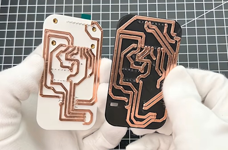
Custom printed circuit boards have become more and more accessible to the average hobbyist over the last decade. But one problem still remains: your circuits will take at least a couple days to make. But what if you needed some really rapid prototypes? [The Raccoon Lab] shows us how to do it with a 3D printer.
You start with the usual hobby PCB pipeline: take your idea, make a schematic, and then lay it out in KiCad. That’s where the changes start: to keep traces strong, they are made very thick. The PCB is then exported and opened in 3D CAD software, where the traces are extruded to be 2 mm tall. Off to the printer! The newly printed “circuit board” is made conductive by applying copper tape to it, and traces are cut out along their raised edges.
The result is a very quick and dirty PCB. Sure, it isn’t exactly production-ready, but for just about any simple microcontroller project it’ll do just fine, and it’s a whole lot more accessible than milling one using a CNC! We’ve seen a few variations on this approach recently, including some custom software designed to help along the process.










As already mentioned in the first comment in the article from 2026-01-28: It’s silly.
And repeating the hackaday article 4 months later is even sillier, especially when the only “justification” is a 40 seconds youtube short.
I do like Kicad, but for a project like this, building a one-off like this on perf board is quicker. I usually draw the schematic in KiCad, sometimes use the PCB editor to plan footprint layout (footprints on a 2.54mm grid) and then build it on perf board. I use 0.2mm “enameled” copper wire for low current stuff (good for upto 500mA or thereabouts) and thicker wires for higher current stuff.
But this method does make me wonder:
What about using copper tape on some “non conductive” substrate, and then cutting it out with a vinyl cutter? Resolution can probably be a lot higher (I guess down to 500um) And the knife of the vinyl cutter is very thin, so 0.2mm isolation may be doable.
People have actually used Cricuts with actual PCB board directly -the kind used for acid etching or CNC machines. And it works. More info here: https://www.reddit.com/r/electronics/comments/914oa4/singlesided_copper_pcb_cut_with_a_cricut_cutting/
I bet that’s going to dull the blade fast. How many times can you replace the blade on those things without paying the price of a small desktop mill capable of milling PCBs? I’m guessing not many.
The blades are an overpriced wear part, but DIY blades are possible.
The challenge with the vinyl cutter approach is peeling the off cuts from the board. You’ll spend a lot of time pulling hair-thin strands of copper from the substrate.
Just like last time we had this same article, the better idea is to sink the traces into the substrate and then press the foil into the grooves with a soft rubber pad, then sand off the high spots between the traces.
I’ve also read about using a carbide scribe (conical tip, no “knife” edge) to scratch away the copper. The goal is to make the scratch lines close enough together that the off-cuts get detached completely.
This is done regularly in fablabs, especially for flex pcb prototypes. See this research paper: https://zenodo.org/records/16211947
That is good enough for fee through. For SMD one should use laser printing like in this project https://hackaday.io/project/195654-print-your-own-pcbs-with-laser-or-cnc-or-chemicals
This thread sparked an idea for me. Maybe it has already been done, but sandwiching copper foil between a top and bottom layer of kapton tape should make a quick and dirty flex pcb.
“very” quick ? the tedious work of cutting the copper ? sorry but exposing a PCB to UV, bleaching the resin, rinsing, etching takes me only like 15 minutes, does not take more time if i do a very simple circuit or a much more complex and larger one, is double-sided, and the result is WAY MORE precise and clean.
naive question, where do you rinse the PCB? Is it safe to do it in the normal sewer network?
A perfectly fair question.
Hard no!
Thanks Stephen.
I’m afraid that I’ve seen just too many video (with high view count) where people didn’t give a damn about it. :/
I was contemplating an enamelled copper wire dispenser, maybe using high current to heat it into place or cut lengths as required.
I guess printing a grid of pegs and then giving a 3d printer a wirewrap tool couldn’t be too much of a stretch.
! although I do wonder if some sort of liquid conductor might be a good way to go. Perhaps adding a UV curing polymer. How conductive can nail varnish be made to be.
I guess one of those pen plotter style label makers could be used to cut tinfoil or thin copper sheet.
Maybe the print could have sharp edges and act as a die cutter, lay the foil on top sandwich it and punch out the circuit layout in one go.
I guess there’s nothing stopping you making multiple layer 3DPCBs either.
Robotic wire wrap machines have been built as far back as the ’70-ies. They have been used by IBM and other manufacturers to automate the wiring of the big computers of that era.
For a DIY method, enameled wire could be wrapped around THT dip IC’s or THT resistors, and then cut, followed by an soldering step.
More advanced would be to use ultrasonic welding, similar to how wirebonding machines work on a chip level.
It was (?still is?) called MultiWire. A machine embedded actual wires into the Printed Wiring Board. Because the wires were insulated, like wire wrap, they could be crossed over each other. It was high density back in the 80s.
yes. Also incredibly unreliable. Wires would break in th resin, over time. Perhaps thermal issues. I had a board made in the early eighties. Totally unfit for production.
There are products for hand drawing conductive lines. They aren’t great but they do exist. Non-solderable.
If all you have is a hammer/3Dprinter, then everything looks like a nail/print.
Faster, better, cheaper (yes, all three simultaneously!) techniques include several variants of Manhattan prototyping. What’s not to like?
See examples of many techniques at https://entertaininghacks.wordpress.com/2020/07/22/prototyping-circuits-easy-cheap-fast-reliable-techniques/
Choose whatever combination of techniques and products suits your current job.
I also have a term for the future, PCC (Printed Circuit Cube), where components are crisscross packed together in a three-dimensional cube with printed tracks made of conductive material and air channels maximize cooling exactly where it matters. All printed as the name says.
and makimg repairs that harder in one go.
Not if it’s constructed like Lego.
That’s going to cost a lot in connectors. Good luck 3D printing sense and reliable connectors.
If all you have is a hammer/3D printer, then everything looks like a nail/print. Even amateurs should be aware screws exist!
Faster, better, cheaper (yes, all three simultaneously!) techniques include various forms of Manhattan prototyping. See several examples at
https://entertaininghacks.wordpress.com/2020/07/22/prototyping-circuits-easy-cheap-fast-reliable-techniques/
including SMD components and commercially deliverable prototypes.
Choose the combination of techniques and products that best suit your current job.
And avoid solderless breadboards, unless you enjoy being perplexed by simple circuits such as a one transistor one resistor amplifier.
https://entertaininghacks.wordpress.com/2024/03/16/practical-traps-with-a-one-transistor-audio-amplifier-solderless-breadboards-and-oscilloscopes/
Could you predict that behaviour and its causes?
That oscillator is a good example if you want to understand oscillators / transistors / parasitic inductance but it’s a lousey broadside against breadborads. The circuit is carefully designed to be on the edge of oscillation, and the fact that it “looks simple” doesn’t change that fact. And using deadbug or manhattan is no guarantee that it won’t oscillate, especially depending on your skill at those techniques.
Did you read the whole of both articles, or just part of one?
They note many problems with solderless breadboards that do catch out beginners. They show an example with a trivial circuit that catches out experienced engineers. Did you predict what would happen with an emitter follower amplifier, and the explanations? It was, as noted, sufficiently subtle and unexpected to be mentioned in The Art of Electronics.
They also noted that manhattan isn’t perfect, but gave reasons why they cause fewer problems than typical solderless breadboard construction.
My thought to the questions posed was, CNC milling. That idea was shot down right at the end with the justification that this is “more accessible,” but its also more limited and possibly a bit slower and labor intensive than just milling. A 3D printer is already a CNC, so really it’s a software problem to say that 3D printing is more accessible. Especially if you can reach higher density with a mill, a single sided board even with a few jumpers would be easier to make than this type of 3D printed board.
On an unrelated note, I’m sure tired of seeing people wear stupid gloves to do things that absolutely do not require gloves. The black latex is dumb enough, but these fuzzy white gloves ratchet everything up to Mickey Mouse level insanity. Can we just stop pretending to be pros and do pro level work instead?
but… I like Micky Mouse.
Would you like me to remedy that for you?
I remember Project Binky, they made a custom “3D printer” that printed PCBs.
It printed PCB traces made of tin on a suitable substrate.
Nah I’d rather just make one in an hour with regular print to double OH paper use positive photo resist and transfer the layout to the resist wash it in NaOH and then just etch with ferric chloride. Easier.
This is how I still do it, but I use ammonium persulphate instead of ferric chloride. You can see when your board is etched , which is more difficult with ferric chloride. I have used many techniques to make PCBs, photo etching is the 2nd easiest. The 1st being to mill as you can cnc drill the holes as well, which is one of the most annoying parts. I’ve laid down tape, I’ve used dalo pens, I’ve burnished on donuts. I’ve been doing this for 45 years. I need to build a cnc mill.
When I worked in the PCB industry in the ’80’s, drilling was 90% of the time, expense, hassel, headaches, you name it. One day, long after I had left the industry, I was making a one-off board for a hobby project, and I got one of those blinding flashes, or maybe it just a dull thud. I reversed the artwork, drew it onto the board with a Sharpie, like I do with all my one-offs, etched in ferric, and soldered the parts right to the foil; Romanian surface mount! I no longer drill, except for board mounting holes. That took the drudgery out of the process, and I found it easier than other wiring techniques.
Interesting; I haven’t heard of that trick before :)
I’ve never managed to get a good etch using Sharpies/Dalo pens.
Just etch your board and be done with it? This seems like so much more work
Where do you buy etchant these days? I still have some from way back when, but who stocks it theses days?
It took all of 20 seconds to find ferric chloride for $53 a gallon on Amazon. Smaller sizes for smaller prices.
I make my own; muriatic acid (hydrochloric acid) and hydrogen peroxide.
Amazon and Ebay both have vendors selling ammonium persulfate — as Dave Everett points out above, it’s nice because you can watch the process. And it’s less messy than ferric chloride. Amazon is considerably less expensive, $25 for 2 lb, with free shipping. However I’d be willing to bet long odds that it is not packaged as hazmat. That’s more of a problem for the vendor than the buyer, if a package bursts open during shipping…
Unsure how a CNC mill is inaccessible when a 3018-class machine is about the same cost as a printer. This definitely fits into the “When all you have is a hammer, everything looks like a nail” category. And that’s coming from someone whose printer sits next to their desktop CNC on the workbench.
Wow! I was for sure that you were full of it, because 3D printers are absurdly inexpenive these days. But, lo!, google “cnc 3018” and there’s a large collection of 3-axis mills in the “around $200” family, which all look sufficient for rough pcb work! thanks!
Can even do CNC furniture with them.
For dollhouses?
My 3018 is a lot of fun to use. I got it for about $200 and I bought a few upgrades as well. All in, less than $300 for 2 sided pcbs on demand. Not bad. I need to figure out some solder mask techniques though, cause some of the finer pitch chips are just a pain to solder, even with isolation routing. Maybe I need to increase my isolation margins.
There is a “mess factor” that you don’t get with a 3d printer. CNCing and SLA printing really need a dedicates space, or garage. I find soldering in the office borderline acceptable. Next house, heated garage.
I can see this making sense to someone in a student single room situation. Something you can do where you sleep.
But, I would not use this. This looks so crude, a strip board has more detailed traces. Also wastes a lot of copper foil. PLA circuit board might deform, if you print in ABS you don’t want to sleep there.
If one wanted to do a 3D printer (because maybe you don’t have a CNC or Circuit), I bet the following combination of known techniques would work well:
Print with the traces RECESSED about half a millimeter or more. Holes can be included, and you could even do double sided if the bottom layer traces are angled grooves.
Brush (temporary) conductive paint mostly into the grooves
Sand for a few seconds to remove excess paint that is outside of the grooves / traces
Electroplate with a glass of vinegar and household battery. Electroplating with copper is easy — I did it when I was a small child. I ended up with a copper-plated quarter and a nickel-plated penny when they swapped metals.
That will even plate your through holes.
Yah, I see this electroplating idea come up a lot when the conversation turns to easy-bake PCBs.
But doesn’t that mean you have to run a conductor to every trace? That’s might not be too bad for a really simple circuit. But if you are building something so simple then why not just use stripboard or perfboard?
I guess you might be able to include temporary jumpers shorting all the traces that you grind off later. But even then, that sounds pretty tedious for any project complex enough to be worth makin a pcb.
Thinking this through… I always come to the thought… if you tried to arrange your parts so that you have lots of parallel traces going all the way to an end of the board you could have a shorting trace along the edge that is a simple trimming step to remove.
And then I remember that is just re-inventing the stripboard but badly.
That’s a great point. With a simple solution, perhaps.
Above, I wrote:
Paint
Sand
Plate
Perhaps swap that:
Paint
Plate
Sand
While doing the “temporary” conductive paint, have each trace connected to one you did earlier.
Meaning it’s connected by a paint going over the ridge.
Then AFTER plating, three seconds on the belt sander or 30 seconds with a sanding block will remove the now-plated extra paint.
That might work. Or the metal might be better attached to itself than the plastic causing your traces to rip out as the unwanted metal is sanded off. I guess one would have to try.
At this point though would such a solution really be any easier than the old traditional acid etching of a blank PCB? Potentially staining liquid.. check. Lots of post processing… check.
How would this home plating compare in thickness, consistency or adherence to the board?
Don’t get me wrong… I think it would be great to see someone do this and write it up or make a video so we can see what can be learned from the experience. But I have a lot of doubts about it actually being as good as more traditional methods, neither in easiness/convenience nor final outcome.
It seems workable but fwiw you really have to tune your printer/slicer specifically for uh i’m gonna call them “canals”. In my printer, a half milimeter canal is good enough to be legible but it might require some x-acto knife sort of post processing to use it for a circuit. And depending on your filament, that sanding step might not go as you imagine. I know i’ve definitely used PLA where if there are any peaks in the top layer (and there always are), you will smear those around instead of sanding off the paint just below.
All seems pretty fiddly to me. Especially when i remember that the one time i used plastic to fix wires in position, it deformed horribly when i soldered :)
Good point about the melting. Soldering is going to melt the plastic that is holding the traces together.
Nah. we have already seen similar methods here on HaD and they addressed that. The key was not lingering on any one connection with the soldering iron for too long.
I’d imagine that if you have parts that have a lot of pins that are close together like ICs or long pin headers you would need to stagger which pin you solder so you aren’t soldering two pins that are near each other one right after the other. That’s good practice anyway but it might be more important with this method . You might even have to pause between some of them to allow the ‘board’ time to cool.
OTOH… I’m not sure this method is going to be good for making traces thin and close spaced enough for this to be a problem. Which kind of comes back to my idea that if your project is simple enough to use this method you ought to just go buy some strip, vero or perfboard.
Does anyone know what’s in this stuff? https://caswellplating.com/plastic-activator-for-electroless-nickel/
if it’s already being printed why not print grooves that can be filled with low temp paste and baked? I guess for FDM printers heat would be a problem, but using MSLA the resins can take quite a bit of heat.
if it’s just for quick prototyping a quick spray of shellac should be more than enough to hold them in place after baking long enough for testing.
Since I saw Polymatt building his own in the custom PSP video (https://www.youtube.com/watch?v=ORz3dcgBAVE), I’ve been thinking about it, but it still feels like the early days of 3D printing and I don’t think I have the patience to jump in that early anymore.
Looks like a lot of work, but I don’t think the idea is totally without merit. Any thoughts on the idea of 3D metal printing?
I thought that someone had started to sell conductive printer filament
Well there is already Proto-Pasta Conductive PLA:, more like printable resistors, but anyway.
If you are dead set on using a 3d printer , how about printing resist onto a circuit board and etching it? It’s got to be faster and easier, maybe even cheaper,
If there is some problem with 3d filament not holding up to ferric chloride, zip tie a resist pen to the print head.
Or use a resist pen in a vinyl cutter / pen plotter.
Or conductive ink in any of those resist pen scenarios.
I used to do fine art print making and it’s dead simple to etch copper. Covering yourself in Vaseline and rolling around on a copper or zink plate and sloshing it in acid or ferric chloride is probably done at every art school as soon as the students forget about the last time someone did it.
Or you could just by a cheap smal cnc-mill of ebay, a few cheap tools, configure surface maping and mill from blanks.
Prototyping one breadboard ofc.